
Op-amp gain
An op-amp gain stage. The Simple view gives the gain, the noise gain, the bandwidth and the input impedance of an inverting, non-inverting, difference or summing stage, with resistor pairs for a target gain. The Advanced view checks the whole stage with a real op-amp: output swing and input range, slew rate and flatness, phase margin with a capacitive load and the isolation resistor, the DC error budget over temperature, noise, the step response and the tolerance, and it picks the op-amp from the library’s 5,872 usable models. Group Parts. Search words include op amp, operational amplifier, gain, inverting, non-inverting, difference, summing, gbw and feedback.
The window, the Simple and Advanced views, full screen and the place buttons are in The calculator window.
56.1Simple: gain and bandwidth
| Choice | Options | What it does |
|---|---|---|
| Stage | Inverting, Non-inverting, Difference, Summing | |
| Resistor series | E12, E24, E96 | Shown while Rf is solved. |
| Field | Unit | Default | What it does |
|---|---|---|---|
| Target gain | V/V | 10 | Shown while Rf is solved. Inverting and difference stages give 0 or more, non-inverting 1 or more. |
| R1 | Ω, kΩ, MΩ | 10 kΩ | The input resistor (non-inverting: the resistor to ground). |
| R2 | Ω, kΩ, MΩ | 10 kΩ | Summing: the second input resistor. |
| Rf | Ω, kΩ, MΩ | 100 kΩ (solved) | SOLVE, solved when the calculator opens. In the difference stage R4 has the same value. |
| Gain-bandwidth product | kHz, MHz | 1 MHz | Reads a selected op-amp’s gbw. |
| Open-loop DC gain | V/V | 100000 | Reads a selected op-amp’s gain. |
| Supply, plus and minus | V | 15 | Sets the rails of the placed circuit (at least ±3 V). |
Inverting G = −Rf/R1 and Zin = R1. Non-inverting G = 1 + Rf/R1. Difference Vout = Rf/R1 (V+ − V−) with R3 = R1 and R4 = Rf, Zin = 2 R1. Summing Vout = −Rf (V1/R1 + V2/R2). The noise gain NG = 1 + Rf/R1 (summing 1 + Rf/(R1 ∥ R2)), the bandwidth fc = GBW / NG (single pole), and H(f) = G / (1 + NG/Aol(f)).
| Result | What it is |
|---|---|
| Gain, Gain in dB | Negative for inverting and summing (orange). |
| Gain from input 2 | Summing. |
| Rf exact, Rf nearest E24 | When Rf is solved: the nearest value and the gain it gives. |
| Noise gain, Bandwidth (−3 dB), Input impedance | Non-inverting: the op-amp input, very high. |
| DC gain error | NG / Aol. |
With Rf solved, a table Closest E24 pairs lists the six pairs (R1 from 1 kΩ to 100 kΩ) with the smallest gain error. The Closed-loop response plot marks the −3 dB point and the GBW.
| Message | When it shows |
|---|---|
| "A non-inverting stage cannot have a gain under 1." | Target under 1 (Rf is then set equal to R1). |
| "A resistor under 1 kΩ loads the output hard. Scale both resistors up by the same factor." | R1 or Rf under 1 kΩ. |
| "A resistor over 1 MΩ adds noise and makes the input bias current matter. Scale both down." | Over 1 MΩ. |
| "The bandwidth is 9.01 kHz. A signal near it loses gain and shifts in phase. Use an op-amp with more gain-bandwidth." | Bandwidth under 20 kHz. |
| "The finite open-loop gain costs … % of the gain. Use an op-amp with more DC gain or a lower stage gain." | DC gain error over 1 %. |
| "R1 and R2 differ by 900 %. Input 1 is weighted −100 V/V and input 2 −10 V/V. Use equal resistors for an equal sum." | Summing with R1 and R2 more than 50 % apart. |
| Button | What it does |
|---|---|
| Place and run AC | U_OA (gbw and gain from the fields) on ± rails, R1_OA and RF_OA (R3_OA, R4_OA for a difference, R2_OA and a second source for summing), a 10 kΩ load, a 1 kHz source, OUT probed, an AC sweep at 20 points per decade. Gain within ±0.1 dB and Bandwidth (bw3db) within ±10 % of fc. |
| Apply to the selected resistors | Sorted by name: R1, Rf (summing R1, R2, Rf). |
- Open the op-amp gain (type
op amp): inverting, target 10, R1 10 kΩ, GBW 1 MHz. - Switch Stage to Non-inverting and press Place and run AC.
You should seeInverting: −10 V/V (20 dB), Rf 100 kΩ, noise gain 11, 90.9 kHz, Zin 10 kΩ, 0.011 % gain error. Non-inverting: Rf exact 90 kΩ, nearest E24 91 kΩ (10.1 V/V), and the pair 3 kΩ and 27 kΩ gives exactly 10. The run reads 20 dB and 100 kHz and both pass.
56.2Advanced: the real stage
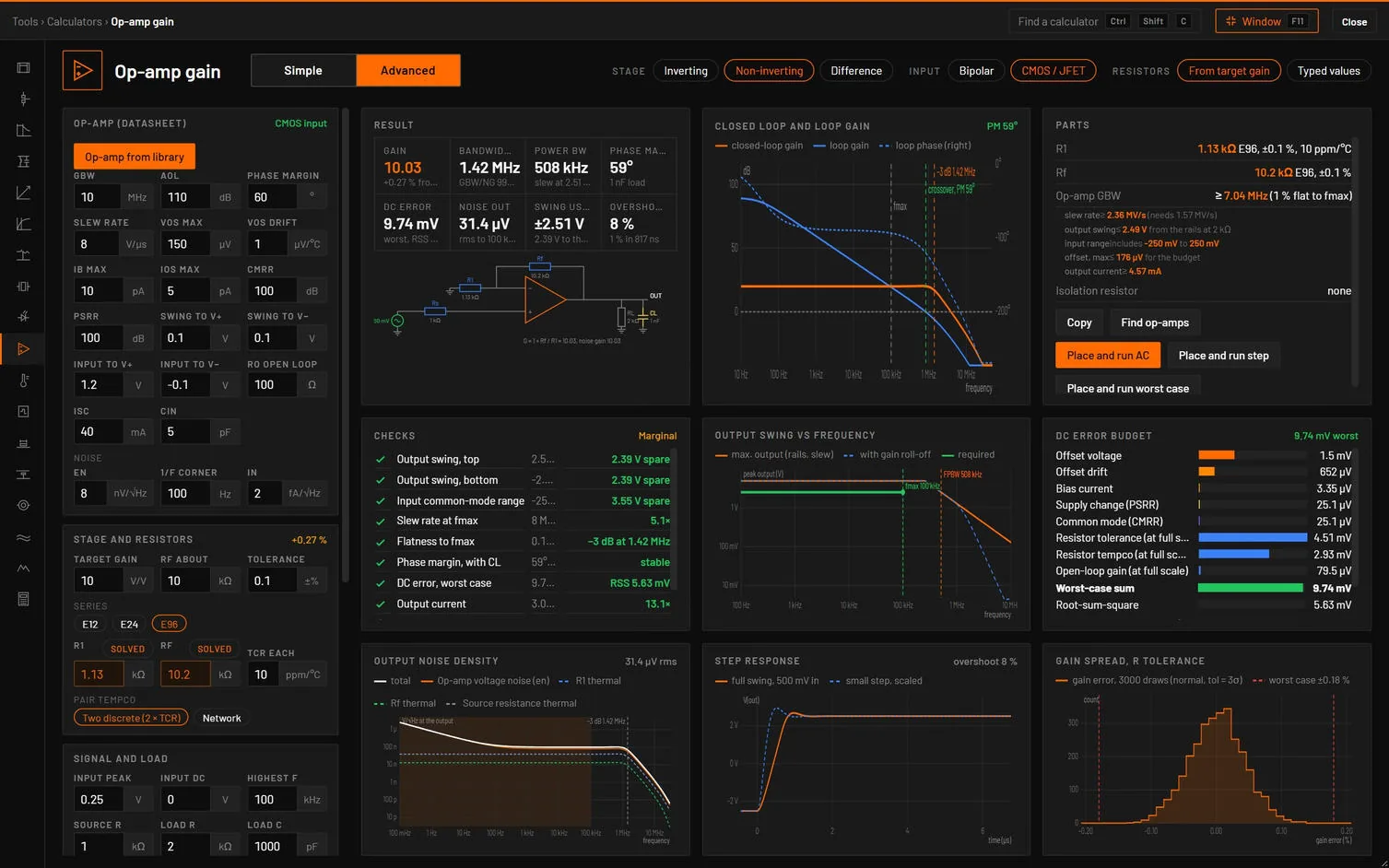
| Choice | Options | What it does |
|---|---|---|
| Stage | Inverting, Non-inverting, Difference | The Advanced view has no summing stage: choosing Summing in the Simple view leaves the Advanced stage as it was. |
| Input | Bipolar, CMOS / JFET | How the bias current changes with temperature. |
| Resistors | From target gain, Typed values | From target gain picks R1 and Rf from the series (SOLVED). Typing R1 or Rf switches to Typed values. |
| Tab | Its dot | Cards |
|---|---|---|
| Design | The worst check. | Result, Stage, Checks, Parts, Output swing vs frequency. |
| Bandwidth and stability | Green with a phase margin of 45° or more, amber 30° or more, else red. | Closed loop and loop gain, Step response, Stability. |
| DC accuracy | Green when the worst-case DC error is within the limit, else amber. | DC error budget, Gain spread. |
| Noise | Green with an SNR of 90 dB or more, else amber. | Output noise density, Noise by source. |
| Verify in simulation | None. | Calculator vs simulation. |
| Field | Unit | Default | What it does |
|---|---|---|---|
| Op-amp from library | Group Op-amp: opens the picker. With a part chosen: its name, input type and rating, how its vendor model runs, and Change, Typed values, and Est. max or Typical for the worst case. | ||
| Target gain, Rf about, Tolerance | V/V, kΩ, ±% | 10, 10, 0.1 | Group Stage and resistors. Its badge is the gain error of the standard parts. The pair search looks for Rf within 3.2 × of Rf about. |
| Series | E12, E24, E96 | ||
| R1, Rf | kΩ | SOLVED | |
| TCR each, Pair tempco, Tracking | ppm/°C | 10, Two discrete (2 × TCR) or Network, 5 | |
| R, + input | kΩ | 0 | Inverting: a resistor from + to ground that cancels the bias current (0 = grounded). |
| Input peak, Input DC (Input CM), Highest f | V, V, kHz | 0.25, 0, 100 | Group Signal and load. |
| Source R, Load R, Load C, Riso, Cf across Rf | kΩ, kΩ, pF, Ω, pF | 1, 2, 1000, 0, 0 | With an inverting or difference stage the source resistance is part of R1. |
| V+, V−, Reference, Supply change | V | 5, −5, 0, 0.25 | Group Supply, temperature, budget. |
| T min, T max, DC error limit (out) | °C, °C, mV | −40, 85, 10 | |
| GBW, Aol, Phase margin, Slew rate | MHz, dB, °, V/µs | 10, 110, 60, 8 | Group Op-amp (datasheet), or Op-amp, fields from the part (marked PART). |
| Vos max, Vos drift, Ib max, Ios max | µV, µV/°C, pA, pA | 150, 1, 10, 5 | |
| CMRR, PSRR | dB | 100, 100 | |
| Swing to V+, Swing to V−, Input to V+, Input to V− | V | 0.1, 0.1, 1.2, −0.1 | The output’s distance from each rail at the load, and the input range (here −5.1 V to 3.8 V). |
| Ro open loop, Isc, Cin | Ω, mA, pF | 100, 40, 5 | |
| en, 1/f corner, in | nV/√Hz, Hz, fA/√Hz | 8, 100, 2 | |
| Integrate, From, Monte Carlo distribution | Signal band (to fmax) or Full bandwidth, 0.1 Hz, Normal or Uniform | Group Noise band. |
How it works it out. The stage is solved as a circuit (nodal analysis): the source, Rs, R1, Rf with Cf, Cin on both inputs, the op-amp as a controlled source with two poles (the dominant one at GBW/Aol and a second set by the phase margin), Ro, Riso and the load. That gives the closed-loop gain, the loop gain with its crossover and phase margin (with and without the load capacitance), the −3 dB point, the peaking, and each noise source’s own transfer. The view draws a light pass first and the full one about 20 ms later (190 points, the step, the Riso search and the Monte Carlo), so the overshoot reads … for a moment.
- Resistors: the series pairs with Rf within 3.2 × of Rf about, R1 = Rf/(G − 1) (non-inverting) or Rf/G − Rs, the six with the smallest error, the first used. With an inverting or difference stage the source resistance counts in R1.
- DC error budget, output-referred and worst case over T min to T max (ADI MT-037, MT-038, MT-068): offset, drift, bias current (a CMOS or JFET Ib doubles every 10 °C above 25 °C), PSRR, CMRR, the resistor mismatch for a difference stage, and the gain terms at full scale (tolerance, tempco, open-loop gain, Riso), as a sum and as a root-sum-square.
- Isolation resistor: TI SBOA418’s start value, then a bisection on the circuit for the target margin (60°, or 3° under the margin without the load).
- Noise (ADI MT-049, MT-050): en with its 1/f corner, the current noise at each input, and the thermal noise of each resistor, each through its own transfer, integrated over the band with no 1.57 factor.
- Gain spread: 3000 draws of R1 and Rf. Step: the same circuit integrated with the slew rate and the swing limits, a small and a full step.
| Result | What it is |
|---|---|
| Gain | Of the standard pair, and how far from the target. |
| Bandwidth | −3 dB, and GBW/NG. |
| Power BW | Slew rate over 2π × peak. Red below the highest frequency. |
| Phase margin | With the load capacitance. Amber under 45°, red under 30°. |
| DC error | Worst case, and RSS. Amber over the limit. |
| Noise out | RMS over the band. |
| Swing used | ± peak, and the room left to the limit. Red when it clips. |
| Overshoot | Of the small step, with the 1 % settling. oscillates when the loop is unstable. |
The Parts card asks for R1 and Rf (series, tolerance, TCR), the bias-cancelling resistor or the matched R3 and R4, the op-amp’s GBW (NG × fmax / 0.1425 for 1 % flatness), slew rate (1.5 × the need), output swing, input range, the largest offset the budget allows, the output current, and the isolation resistor, with Copy and Find op-amps. The Stability table gives the crossover, the phase margin with and without the load, the output pole Ro·CL, the input pole, the Riso start value (TI SBOA418) and the Riso for the target margin found on this circuit. The DC error budget shows offset terms (orange) and gain terms at full scale (blue).
| Check | Value and limit | Passes | Marginal | Fails |
|---|---|---|---|---|
| Output swing, top (and bottom) | output · limit | 0.1 V spare or more | 0 to 0.1 V | Clips |
| Input common-mode range | range · allowed | 0.1 V spare or more | 0 to 0.1 V | Outside |
| Slew rate at fmax | SR · 2π fmax Vo | 1.5 × or more | 1 × or more | Less |
| Flatness to fmax | gain change | Within 1 % | Within 10 % | More |
| Phase margin, with CL | PM · CL | 45° or more: stable | 30° or more: rings | Less: unstable |
| DC error, worst case | error · allowed | Within it | Up to 1.43 × it | More |
| Output current | peak · Isc | 2 × or more | 1 × or more | Less |
| Gain, standard parts | gain · target | Within the tolerance | Within 1 % | More |
| Supply rating (library part) | rating · rails | 1.05 × or more | Equal | Over rating |
| Noise in band | rms · SNR | 90 dB or more | 70 dB or more | Less |
| Message | When it shows |
|---|---|
| "Output range −10 V to 10 V exceeds the swing −2.9 V to 2.9 V at 600 Ω. Lower the gain or the input, or use a rail-to-rail output." | The output clips. |
| "Input common mode … is outside the input range …. The output distorts or phase-reverses. Move the bias point or use a part whose input range includes that rail." | Outside the input range. |
| "A 10 V peak sine at 200 kHz needs 12.6 MV/s. The part slews 2 MV/s, so the output is slew-limited above 31.8 kHz. Use a faster part or keep the swing under 1.59 V peak." | Slew-limited. |
| "Phase margin 29° with 100 nF (89° without). Small-step overshoot 42 %. Riso 39 Ω between output and capacitor gives 60° (SBOA418 start value 6.11 Ω)." | Margin under 45° (or: Raise the noise gain or reduce CL.). |
| "The rails span …, above the … V rating of the part. Lower the rails or pick a part rated for them." | A library part rated below the rails. |
| "R1 20 Ω is below the source resistance 1 kΩ, so the source sets most of the gain. Raise Rf about to 100 kΩ or more." | Inverting with R1 under Rs. Otherwise with Rs: Rs … is in series with R1 and sets part of the gain. |
| "Bias current is a large share of the error. Add … (R1 ∥ Rf) in series with the + input to cancel Ib. Ios remains." | Bipolar input. |
| "A resistor above 1 MΩ adds noise, and with Cin it puts a pole near the crossover. Scale both resistors down." | |
| "No resistor pair for gain …. A non-inverting stage has a gain of at least 1. Typed values shown." |
56.3The op-amp picker
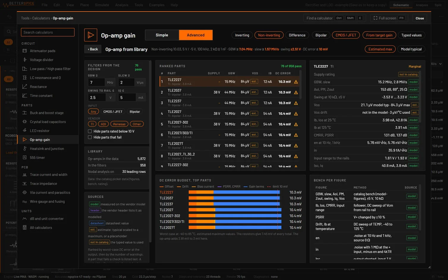
Open it with Op-amp from library, Find op-amps on the Parts card, or Change. The head shows what the stage needs (Non-inverting 10, 5 V / −5 V, 100 kHz, 2 kΩ ∥ 1 nF · GBW ≥ 7.04 MHz · slew ≥ 1.57 MV/s · swing ±2.51 V · DC error ≤ 10 mV) and Worst case from: Estimated max or Model typical.
The data. The catalogue has 6,278 op-amp models. The 5,872 with a gain-bandwidth figure are in the picker: TI (with Burr-Brown and National) 2,589, ADI (with Linear Technology and Maxim) 2,302, Renesas (Intersil) 279, others 702. GBW, slew, Aol, phase margin, Zout, swing, Iq and Vos come from the catalogue’s bench on each vendor model at ±5 V into 10 kΩ. 5,278 also have figures measured on the vendor model with ngspice for this picker: Ib and Ios, CMRR and the input range (a DC sweep of the common mode), PSRR (V+ changed by ±10 %), drift and Ib at temperature (a sweep from −40 to 125 °C), en at 10 Hz and 1 kHz, in, and Isc. 1,665 have a supply rating from the datasheet or ti.com page. The Bench per figure card lists how each figure was measured.
| Field | Unit | Default | What it does |
|---|---|---|---|
| GBW ≥ | MHz | NG × fmax / 0.1425 (7 MHz here) | Group Filters from the design, badge the number that pass. The four numbers follow the design until you type in one. |
| Slew ≥ | V/µs | 1.25 × the need (2 V/µs here) | |
| Swing to rail ≤ | V | the room to the rails (2.5 V here) | The part’s output swing to a rail, from its ±5 V bench. |
| Iq ≤ | mA | 5 | A part with no Iq passes. |
| Input | Any, CMOS / JFET, Bipolar | From the part’s Ib: under 1 nA is CMOS / JFET. | |
| Vendor | TI, ADI, Renesas, Other | ||
| Hide parts rated below 10 V, Hide parts that fail | off |
The Library card counts Op-amps in the data (5,872), In the filters (958 for the default stage) and Nodal analysis on 30 leading rows.
How the ranking works.
- Filters. Every usable part is tested against GBW, slew, Iq, vendor, swing to the rails, and the rating if that box is ticked.
- Closed forms on every part that passes the filters. The part’s figures replace the typed ones and the stage is worked out with the same R1 and Rf for every part: output swing, input range, slew rate, the DC error budget, output current, supply rating. A figure the catalogue doesn’t have is filled, for the ranking only, with the worse of your typed value and the library’s 90th percentile, and the part is listed after every part that has all its figures. A part fails when any of these checks fails.
- Order. Passing parts first, then parts with every figure, then the smallest worst-case DC error at the output, then the fewest warnings.
- Nodal analysis on the leading 30. The first 30 rows (and the selected one) are solved again as a circuit, which adds the phase margin with the load, the noise and the flatness, and are sorted again.
The table shows the 30 analysed rows: the part (vendor group, input type, Iq), its supply rating (red below the rails), GBW, Vos, Ib, the worst-case DC error (with a gaps tag when a figure was filled in) and the status. Full screen adds the slew rate, en at 1 kHz, the phase margin with the load, the output noise and how its vendor model simulates. Hovering a row names its failed or marginal checks. The 30 are a view, not a limit: every part in the filters is ranked, so narrow the filters to bring a part into the 30.
Use this part fills the op-amp fields (marked PART) from the part: GBW, Aol, phase margin, slew rate, Ro, swing and input range, Isc, en, the 1/f corner, in and the input type as measured (tag model), and the rating (datasheet or header). With Estimated max the typical model values are scaled to an estimated maximum until the catalogue holds the datasheet maxima: Vos × 4, drift, Ib and Ios × 3, CMRR and PSRR − 10 dB (tag est.). A figure the model does not give gets a placeholder and a note: 3 mV offset, 3 µV/°C drift, 20 nV/√Hz noise, 80 dB PSRR. The detail card lists every figure with its source, four tiles (DC error, noise, phase margin, swing spare), Show what is placed and Place with this model. DC error budget, top parts compares the seven best.
56.4Verify in simulation
| Check | Analysis and measurement | Limit |
|---|---|---|
| Gain at 1 kHz | AC, gain of V(OUT) at min(1 kHz, f3/100) | ±0.1 dB |
| −3 dB bandwidth | AC, bw3db of V(OUT) | ±3 % |
| Phase margin | Loop gain, broken at the output pin | ±1° |
| Output noise | Noise from the From frequency to the band end | ±5 % |
| Overshoot, small step | Transient: a step of 2 % of the swing | ±5 points |
| Rise time, full swing | Transient: the full step (fall time for an inverting stage) | ±15 % |
| Output, worst case | Worst-case operating point with tol on R1, Rf (R3, R4) and vos_max on the op-amp | Every corner inside |
| Button | What it does |
|---|---|
| Place and run AC | A 5-pin op-amp carrying every datasheet value (gbw, gain, pm, slew, vos, vos_tc, ib, ios, cmrr_db, psrr_db, rail and input-range limits, rout, isc, cin, en, en_fc, inoise) on V+ and V− flags, the source behind Rs, R1 and Rf (Cf) with tol and tc1, RL and CL behind Riso, and an AC sweep at 40 points per decade. Gain and Bandwidth. |
| Place and run step | A small step then a full step. Overshoot, small step and Rise 10-90 %, full step. |
| Place and run worst case | A DC input of the peak, tol on the resistors and the offset at ±Vos max (bias currents off), a worst-case run of 200 (seed 1). Output, worst case. |
| Place circuit | The stage only. |
| Place with OPA197 | With a library part: its vendor model instead of the datasheet values, and an AC run. Its gain follows the calculator. Its bandwidth and margin come from the vendor model’s own poles. |
| Apply to selection | R1 to the first selected resistor, Rf to the second. |
The drift, bias current, PSRR and CMRR terms of the budget stay calculator only.
| Simple | Advanced |
|---|---|
| Target gain, R1, Rf, Gain-bandwidth product | Target gain, R1, Rf, GBW (when typed) |
| Open-loop DC gain | Aol in dB |
| Supply, plus and minus | V+ and V− |
| Stage, Resistor series | Stage (not Summing), Series |
- Open the op-amp gain and press Advanced: non-inverting, 10, E96 ±0.1 %, ±5 V, 250 mV peak to 100 kHz, 2 kΩ and 1 nF, GBW 10 MHz.
- Press Op-amp from library, select OPA197 and press Use this part.
You should seeR1 1.13 kΩ and Rf 10.2 kΩ give 10.03 (+0.27 %, amber against ±0.1 %). Bandwidth 1.42 MHz, phase margin 59° with 1 nF (85° without), DC error 9.74 mV worst (RSS 5.63 mV) against 10 mV, noise 31.4 µV (SNR 95 dB), overshoot 8 %. The picker has 958 parts in the filters and 76 pass. With OPA197 the margin drops to 41° (rings, Riso 160 Ω suggested) and the DC error rises to 38 mV: its model has no offset, so the 3 mV placeholder × the noise gain fails the budget until the datasheet maximum is typed.
Sources. Horowitz and Hill, The Art of Electronics chapter 4, ADI MT-049 and MT-050 (noise), MT-037, MT-038 and MT-068 (DC errors, difference amplifier), TI SBOA418 (isolation resistor). The tests check the single-pole stage, the noise against MT-049, a two-pole buffer’s 6.4 % overshoot, the Riso search, the budget terms, the E96 pairs against every pair, the picker’s gap handling, and the placed stages (AC, loop gain, noise, step, worst case, and the vendor models of OPA197, OPA2156 and OPAx211 within 0.05 dB) against bspice.