
Buck and boost stage
The power stage of a buck (step-down) or boost (step-up) switching converter. The Simple view gives the duty, the inductor for a ripple, the peak and valley current, the output capacitor and the CCM boundary, and places an ideal-switch stage. The Advanced view designs the whole stage over the input range: three peak currents (full load, current limit, start-up), the inductor’s saturation and heat, the capacitors after DC bias, every loss, the power stage response, the frequency trade, and real parts picked from the library (6,223 power inductors and 649 TI switching regulators). Group Parts. Search words include buck, boost, inductor, smps, switching, regulator, ripple, ccm, dcm and converter.
The window, the Simple and Advanced views, full screen and the place buttons are in The calculator window.
58.1Simple: the ideal stage
| Choice | Options | What it does |
|---|---|---|
| Stage | Buck, Boost | Loads starting voltages: buck 12 V to 5 V, boost 5 V to 12 V. |
| Rectifier in the placed circuit | Synchronous switch, Diode | With a diode its forward drop enters the duty and the placed stage has a Schottky diode. |
| Field | Unit | Default | What it does |
|---|---|---|---|
| Input voltage, Output voltage | V | 12, 5 (boost 5, 12) | 0.5 to 1000 V. |
| Output current | mA, A | 2 A | |
| Switching frequency | kHz, MHz | 500 kHz | 1 kHz to 20 MHz. |
| Inductor ripple | % | 30 | Peak to peak, of the average inductor current. 20 to 40 % is usual. Shown while Inductance is solved. |
| Inductance | nH, µH, mH | 10 µH (solved) | SOLVE, solved when the calculator opens. Typed: used exactly. |
| Output ripple allowed | mV, V | 20 mV | Peak to peak. |
| Capacitor ESR | mΩ, Ω | 10 mΩ | |
| Diode forward voltage | V | 0.4 | Diode rectifier: the drop at the load current (a Schottky is 0.3 to 0.5 V). |
| Efficiency | % | 100 | 100 for the ideal stage the placed circuit builds. |
Buck: D = (Vout + Vd) / (η Vin + Vd), ΔIL = (Vin − Vout) D / (fs L), L = Vout (Vin − Vout) / (ΔIL fs Vin), Ipk = Iout + ΔIL/2, Cout = ΔIL / (8 fs (ΔV − ESR ΔIL)), Icrit = ΔIL/2. Boost: D = (Vout + Vd − η Vin) / (Vout + Vd), ΔIL = Vin D / (fs L), Iin = Iout / (1 − D), Ipk = Iin + ΔIL/2, Cout = Iout D / (fs (ΔV − ESR Ipk)), Icrit = (1 − D) ΔIL/2. A solved L is rounded up to the next E6 value (3 % slack) and the stage is worked out with it. The capacitor is the next E12 value up.
| Result | What it is |
|---|---|
| Duty cycle | Orange. |
| Inductance, exact and Inductance, E6 | When solved (else Inductance). |
| Inductor ripple current, Peak inductor current, Valley inductor current | |
| Output capacitor, minimum and E12 | ESR too high when the ESR alone uses up the ripple. |
| Output ripple with that capacitor | The capacitor current integrated over a period plus the ESR step. |
| Ripple, datasheet worst case sum | The two terms added. |
| CCM boundary (load current), Mode at this load | CCM, DCM (diode), or CCM, I(L) < 0 (synchronous in forced PWM). |
| Diode average current (buck), Input current (boost) |
The plots Inductor current and Switch node show two periods.
| Message | When it shows |
|---|---|
| "A buck stage needs an output voltage below the input. Lower the output or raise the input." | Buck with Vout ≥ Vin (boost likewise). No results. |
| "Duty is 98 %, above 95 %. Controllers cannot make an off-time that short, and losses limit the step-up. Lower the step-up ratio or use two stages." | Duty over 95 %. |
| "ESR ripple alone is 58.3 mV, over the 20 mV allowed. Use a capacitor with lower ESR or allow more ripple." | No capacitor can meet the ripple. |
| "Load current 50 mA is below the CCM boundary of 3.05 A. The stage runs in discontinuous mode and the duty and ripple equations do not hold. Raise the inductance or the frequency." | Diode, below the boundary. |
| "Load current 50 mA is below the CCM boundary of 2.92 A. With a synchronous switch in forced PWM the inductor current goes negative to −2.87 A and the stage stays in CCM. The light-load loss stays high. Raise the inductance or the frequency, or use diode emulation." | Synchronous, below the boundary. |
| "Ripple current is … % of the average current. The CCM boundary is at … % of the load, so light loads drive the inductor current negative. Raise the inductance." | Ripple over 120 %. |
| "Ripple current is under 10 %, which needs a large inductor. 20 to 40 % is usual." | Ripple under 10 %. |
| "The duty includes the efficiency set above, so it is a little above the ideal ratio." | Efficiency under 100 %. |
| Button | What it does |
|---|---|
| Place and run a transient | An ideal-switch stage: V_IN_PS, the switch S_HI_PS driven by a PWM source at D, S_LO_PS with an inverted PWM (or a Schottky D_PS), L_PS (starting at its average current), C_OUT_PS with its ESR (starting at Vout), R_LOAD_PS = Vout/Iout, OUT, and probes V out, I L_PS, V sw. A transient long enough for the start-up to ring down (12 RC, 100 to 3000 periods), measured over the last 20 periods: Output ripple within ±15 %, Output mean within ±3 % (diode −10 / +3 %), Inductor ripple current within ±10 %. |
| Apply to the selected inductor and capacitor | The L used and the E12 capacitor into the selected parts. |
- Open the buck and boost stage (type
buck): 12 V to 5 V, 2 A, 500 kHz, 30 % ripple, 20 mV, 10 mΩ. - Press Place and run a transient.
You should seeD 41.67 %, L 9.722 µH exact, 10 µH E6, ripple 583 mA, peak 2.292 A, valley 1.708 A, Cout at least 10.29 µF so 12 µF, output ripple 12.88 mV (17.99 mV as the worst-case sum), boundary 292 mA, CCM. The run measures 10.94 to 14.81 mV ripple, 4.85 to 5.15 V mean and 525 to 642 mA inductor ripple, and all pass.
58.2Advanced: the whole stage
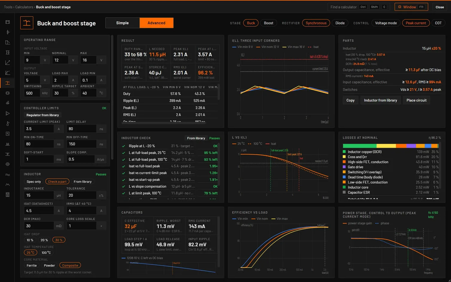
| Choice | Options | What it does |
|---|---|---|
| Stage | Buck, Boost | Resets the operating range, controller, inductor and capacitor groups to that stage’s starting values and clears a chosen regulator. The switches stay. |
| Rectifier | Synchronous, Diode | |
| Control | Voltage mode, Peak current, COT | Sets the response model and the slope compensation check. |
| Tab | Its dot | Cards |
|---|---|---|
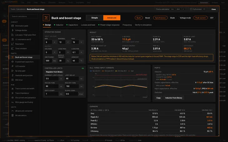
| Design | Amber with a warning. | Result (with the corners, checks and warnings), I(L) three input corners, Parts, Corners. |
| Inductor | The inductor check. | Inductor check, L vs I(L), Corners, Top library parts. |
| Capacitors | Red when the worst ripple is over the limit. | Capacitors. |
| Losses and heat | None. | Losses at nominal, Efficiency vs load. |
| Power stage response | Green. | Power stage Bode plot and Poles and zeros. |
| Frequency | None. | Efficiency and inductor size vs frequency. |
| Verify in simulation | None. | Calculator vs simulation. |
| Field | Unit | Default | What it does |
|---|---|---|---|
| Input voltage Min / Nominal / Max | V | 9 / 12 / 16 (boost 3.3 / 5 / 5.5) | Group Operating range. |
| Output Voltage, Load max, Load min | V, A, A | 5, 2, 0.1 (boost 12, 1, 0.05) | |
| Switching, Ripple target, Ambient | kHz, %, °C | 500, 30, 40 | |
| Current limit (peak), Limit delay | A, ns | 3.5 (boost 6.5), 80 | Group Controller limits. Its badge says OK or 1 problem (an on-time or off-time under the minimum). Regulator from library is here. |
| Min on-time, Min off-time, Soft-start | ns, ns, ms | 80, 150, 1 (boost 2) | |
| Slope comp. | A/µs | 0.5 (boost 0.6) | Peak current control. |
| Inductor source | Spec only, Check a part, From library | Group Inductor. Spec only states a need, Check a part takes a datasheet part, From library opens the picker. | |
| Inductance, Tolerance, Isat (datasheet), Irms (ΔT 40 °C), DCR (max), Core loss scale | µH, ±%, A, A, mΩ, × | 15 (boost 10), 20, 4.5 (9), 4 (7.5), 30 (20), 1 | A library part fills these, marked PART. |
| Isat drop, Isat temperature, Core material | 10, 20, 30 %, 25 °C or 100 °C, Ferrite, Powder, Composite | How the datasheet states Isat, and the core’s roll-off. | |
| C each, Count, Rated, ESR each, ESL each, Ripple max | µF, ×, V, mΩ, nH, mV | 22, 2 (4), 10 (25), 20 (3), 0.4, 20 (120) | Group Output capacitors. |
| Type and size | 0805, 1206 (boost 1210), 1210, Polymer | Sets the DC-bias loss. | |
| Load step, Crossover | A, fs / | 1 (0.5), 10 | |
| C each, Count, Rated, ESR each, Type | µF, ×, V, mΩ | 10 (22), 2, 25 (10), 4, 1206 (0805) | Group Input capacitors. |
| Rds(on) high side, low side, Qg, Qgd, Coss, Gate R, Gate drive, Miller plateau, Dead time, Qrr (or Diode Vf), θJA | mΩ, mΩ, nC, nC, pF, Ω, V, V, ns, nC, °C/W | 18, 8, 8, 2, 300, 2.5, 5, 2.6, 20, 10 (0.4 V), 60 | Group Switches (two FETs), or Switch and diode. |
How it works it out. Everything is at full load and at the three input voltages, with L at its low tolerance for the worst values. The duty includes the losses (solved together with the efficiency). L falls with current along the part’s L(I) curve: a Vishay part’s own tanh law (L/L0 = sech²(I/2a)), a power law through datasheet points, or one rating with the core’s sharpness. The L needed is taken at Vin max for a buck and near ⅔ Vout for a boost (TI SLVA372). The peak at the current limit adds the overshoot of the limit delay, the start-up peak the charge of the output capacitors in the soft-start. Losses: conduction at 1.4 × Rds(on) (about 100 °C), switching (Infineon AN 2006-07), Coss, Qrr, gate drive, dead time or the diode, copper at the DCR’s temperature, a core-loss estimate, capacitor ESR. Output capacitors keep 1 − k (V/Vr)1.25 of their value (k 0.8 for 0805, 0.65 for 1206, 0.5 for 1210, 0 for polymer). The response uses the LC pole, the ESR zero and the boost’s RHP zero, crossover at min(fs/10, RHP/4), and previews the phase margin with a type II or III compensator.
| Result | What it is |
|---|---|
| Duty range | Over the input range. |
| L needed | For the ripple target at the worst corner (orange). |
| Peak I(L), Peak at limit, Peak at start-up | Full load with L at −tolerance, the limit plus its delay, and the soft-start at Vin min. |
| Stored energy (buck) or RHP zero (boost) | ½ L I²pk, or the zero and the crossover it allows. |
| RMS I(L) | Worst corner. |
| Efficiency | At Vin nominal, with the total loss (orange). |
The Corners table gives duty, input current (boost), ripple, peak, RMS, on-time and efficiency at each input voltage, the corner that sets each worst value in orange. The Parts card is what to buy: the inductor (E6 value, Isat at 30 % drop and 100 °C, Irms for a 40 °C rise, DCR for 1 % loss), the output and input capacitance after DC bias with their RMS current, and the switches’ voltage and current, with Copy and Inductor from library. The capacitors card gives C effective, the worst ripple split into its C, ESR and ESL parts, the RMS current, the load step and release, and the input ripple, with a plot of C left against DC bias.
| Check | Value and limit | Passes | Marginal | Fails |
|---|---|---|---|---|
| Ripple at L −20 % | ripple · target | Within 1.25 × target | Up to 1.56 × | More |
| L at full-load peak, 25 °C (and 100 °C) | % left · drop | 80 % or more | 70 % or more | Less |
| Isat vs full-load peak | Isat / peak | 1.2 × or more | 1.0 × or more | Less |
| Isat vs current-limit peak | Isat / limit peak | 1.0 × or more | 0.9 × or more | Less |
| Isat vs start-up peak | Isat / start-up peak | 1.1 × or more | 1.0 × or more | Less |
| L vs slope compensation (peak current) | L · Vout / (2 Se) | 1.1 × or more | 1 × or more | Less: subharmonic |
| RHP zero vs crossover (boost) | RHP zero · fc | RHP/4 ≥ fs/10 | Otherwise: limits fc | |
| L at limit peak, 100 °C | % left | 60 % or more | 45 % or more | Less: runaway |
| Irms rating vs RMS current | Irms / RMS | 1.2 × or more | 1.0 × or more | Less |
| Losses, copper + core | % of Pout | 2 % or less | Up to 3.3 % | More |
| Temperature rise, est. | hot spot | Under 109 °C | Under 125 °C | More |
| Message | When it shows |
|---|---|
| "On-time at Vin max is 61.6 ns, under the 80 ns minimum of the controller. The regulator skips pulses. Lower the switching frequency to 1.39 MHz or less." | On-time too short. |
| "Off-time … at Vin min is under the … minimum. Lower the switching frequency." | Off-time too short. |
| "Isat 2.5 A is below the 6.49 A peak at the current limit. Use a part with Isat ≥ 7.14 A or lower the current limit." | Isat under the limit peak. |
| "Below 248 mA load (the minimum is 100 mA) the inductor current goes negative in forced PWM. The stage stays in CCM and the light-load efficiency drops. Diode emulation or PFM makes it discontinuous instead." | Load min under the boundary (diode: it goes discontinuous). |
| "Output ripple 30.6 mV is over the 20 mV limit. The capacitors keep 84 % of their value at 3.3 V. Add capacitance or use a higher voltage rating." | Over the ripple limit. |
| "Duty goes above 50 % in peak current mode and the slope compensation … A/µs is under the … A/µs needed against subharmonic oscillation. Raise the slope compensation or the inductance." | Peak current mode with too little slope compensation. |
58.3The inductor picker
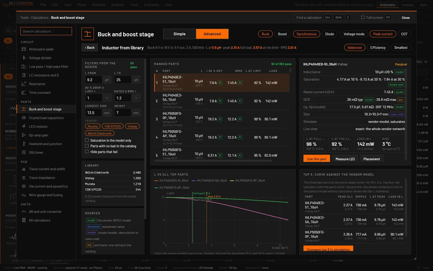
Open it with From library on the inductor check, Inductor from library on the Parts card, Open the library picker under Top library parts, or the inductor source From library. The head shows what the design needs (Buck 9 V to 16 V in, 5 V out, 2 A, 500 kHz · L ≥ 11.5 µH · peak 2.31 A full load, 3.57 A at the limit · RMS 2.01 A) and Rank for: Balanced, Efficiency, Smallest.
The data is the catalogue’s 6,223 power inductors with an L: Würth Elektronik 3,460, Vishay 1,300, Murata 1,219 and TDK EPCOS 244, in 213 families, from 25 nH to 10 H. 3,026 have both a saturation figure and a current rating and can be ranked. The rest are listed only with Parts with no Isat in the catalog. Each part’s saturation comes from the vendor model (Vishay’s tanh law), from datasheet 10 % and 30 % points (Würth and TDK, copied from the makers’ PDFs), or from one rating (Murata’s header Imax, an estimate). The DCR used is the datasheet maximum, else the typical × 1.1.
| Field | Unit | Default | What it does |
|---|---|---|---|
| L from, L to | µH | 0.8 × and 2.2 × L needed | Follow the design until you type in them. |
| 30 % drop ≥ limit × | 1.0 | The part’s current at 30 % drop, at 100 °C, against the peak at the current limit. | |
| Rated ≥ RMS × | 1.2 | Irms against the worst RMS. | |
| Largest side, Height | mm | 13.5, 7 | A part with an unknown size passes. |
| Vendors | all on | ||
| Saturation in the model only, Parts with no Isat in the catalog, Hide parts that fail | off |
Every part in the filters runs the whole design with its own L(I), tolerance, DCR and rating, and gets the full inductor check. A part fails when its 30 % current hot is under the limit peak, its Irms is under the RMS need, its L at the limit peak is under 50 %, or another check fails. Passing parts rank first, then (in Balanced and Smallest) parts with a trusted size, then by a score of loss, temperature rise, footprint and saturation margin weighted by the rank mode. A size that would store more than 8 µJ per mm³ is marked size implausible (a case code read in the wrong unit). The table shows the part (family, size), L, the current at 30 % hot with its source tag, Irms, L at the limit (red under 50 %, orange under 70 %), loss and rise, and in full screen the DCR, the efficiency and how it simulates.
The detail card gives the part’s inductance, saturation points, rating, DCR, Cp and Rp of the model, size, how Simulate and the live view run it, and four tiles (L at full load, L at the limit, loss, rise). Use this part puts it into the design. Measure L(I) places a bench: a 1 A/µs ramp through the vendor model, where V(LI) in volts reads L in µH. Placement shows what the part is placed as: for Würth, the fitted inductor with the datasheet saturation or the vendor model as is (which does not saturate). L vs I(L), top parts plots the best parts at 100 °C, and Top 3, curve against the vendor model compares each with its vendor model as Simulate runs it. Compare top 3 in simulation places the stage three times with the three vendor models and runs one transient with twelve measurements.
58.4The regulator picker
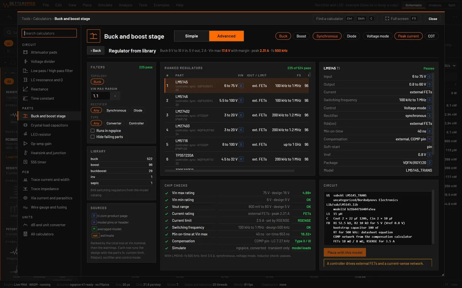
Regulator from library in the Controller limits group lists the catalogue’s TI switching regulators with a known input range: 649 of 727 (buck 522, boost 96, buck-boost 29, inverting and SEPIC one each). The head shows the need with the input margin. Filters: the topology (from the stage), Vin max margin (1.1 ×), Rectifier (Any, Synchronous, Diode), Type (Any, Converter with its own switches, Controller with external FETs), Runs in ngspice and Hide failing parts. The figures come from ti.com product pages (D), the model’s pins or header (H), the averaged model (M) or an estimate.
Each row runs the design with the chip’s switching frequency (fixed, the nearer of two, or the design’s clamped into its range), its current limit, minimum on- and off-time, rectifier, control mode and, for a converter, its Rds(on). Its checks: Vin max and min rating, Vout range, output current rating (1.2 × the load), current limit against the peak (1.2 ×), switching frequency, minimum on-time at Vin max (1.2 ×), compensation, the boost’s RHP zero, and whether the model simulates. A figure the catalogue lacks is amber datasheet. Passing parts rank by the total loss at nominal input plus half a point per marginal check and per PSpice-only model.
Use this part sets those values in the design (shown as PART) and puts the chip in the Controller limits group with Change part and Type values. The Circuit card lists what it would be placed with: the model, the design’s inductor and capacitors, a feedback divider (R2 10 kΩ, R1 for Vout from Vref), bootstrap, RT, COMP network, soft-start, and a Vref field when the catalogue has none. Place with this model places the vendor subcircuit with that stage, pins assigned by their names (VIN, EN, GND, SW, BOOT, FB, COMP, SS, VCC and so on). It says which pins it left open, and refuses with the reason when the pin list, the feedback pin or Vref is missing, or for a controller or a multi-channel part. No analysis runs: a vendor switching model needs Start from initial conditions in the setup and a transient past the soft-start.
58.5Verify in simulation
| Check | Analysis and measurement | Limit |
|---|---|---|
| Output mean | Transient, mean of V(OUT) over the last 20 periods | ±3 % (diode ±6 %) |
| Inductor ripple | Ripple of I(L) | ±10 % |
| Inductor peak | Max of I(L) | ±5 % |
| Output ripple | Ripple of V(OUT) | ±15 % |
| Duty, L at the mean current | Set by the PWM source, and the saturation given to the inductor |
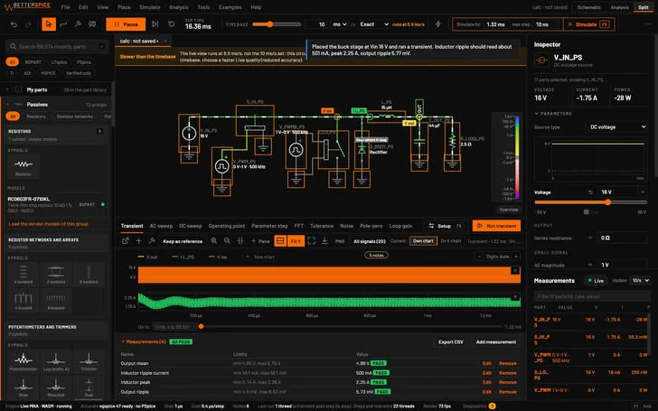
The Corner buttons pick Vin min, nominal or max (default max). The placed stage has ideal switches with Rds(on) (or a Schottky), a body diode for the dead time, the inductor with its DCR and saturation (a typed Isat becomes the simulator’s 50 % point: × 1.53 for a 30 % drop, × 2 for 20 %, × 3 for 10 %, and a library part its own eight-point lisat curve), the output bank as one capacitor with ESR/n and its DC-bias curve, and the load. The duty is found so Vout is right with the conduction drops. The capacitor ESL is left out: its spike is in the Capacitors tab’s ripple.
| Button | What it does |
|---|---|
| Place circuit and run | The stage at the chosen corner and a transient, with the four measurements. |
| Run three corners | The stage at Vin min, nominal and max one under the other (_MIN, _NOM, _MAX), one transient, twelve measurements. |
| Apply to selected L and C | l, dcr and isat (or lisat) into the selected inductor, c, esr and cbias into the selected capacitor. |
| Simple | Advanced |
|---|---|
| Input voltage, Output voltage, Output current, Switching frequency | Vin nominal, Output voltage, Load max, Switching |
| Inductor ripple, Inductance (typed) | Ripple target, Inductance |
| Output ripple allowed, Capacitor ESR | Ripple max, ESR each × count |
| Diode forward voltage, Stage, Rectifier | Diode Vf, Stage, Rectifier |
- Open the buck and boost stage, press Advanced: 9 to 16 V in, 5 V, 2 A, 500 kHz, a 15 µH ±20 % composite inductor rated 4.5 A.
- Open the Inductor tab and press From library. Select the first row and press Use this part.
You should seeThe design: duty 33 to 58 %, L needed 11.5 µH, peaks 2.31 A (full load), 3.57 A (limit), 2.36 A (start-up), efficiency 96.2 % with 399 mW lost (139 mW of it in the inductor’s copper), output ripple 11.3 mV, LC pole 7.27 kHz, crossover 50 kHz, phase margin preview 72.7°. The inductor check passes. One warning: under 248 mA load the current goes negative in forced PWM. The picker lists 362 parts in the window, 93 pass, Vishay IHLP4040ED-51 10 µH first (7.6 A at 30 % hot). With it the ripple at L −20 % reads 46 %: amber, 1.53 × the target.
- Set 9 to 36 V in, 3.3 V, 3 A, 2 MHz, limit 5 A, and the inductor 2.2 µH, Isat 2.5 A, Irms 2.5 A, DCR 60 mΩ.
You should seeThe inductor check fails on ten rows (L falls to 36 % at the peak, Isat is 0.62 × the full-load peak, subharmonic risk, 8.2 % loss), efficiency 80 %. The warnings say the 61.6 ns on-time is under the 80 ns minimum (use 1.39 MHz or less), Isat is under the 6.49 A limit peak (use ≥ 7.14 A), and the 30.6 mV ripple is over 20 mV.
Sources. TI SLVA477 (buck) and SLVA372 (boost), SLVA057 and SLVA061 (DCM, small signal, RHP zero), SLYT670 (input capacitor), Coilcraft Doc 361 and Doc 1733 (Irms as a 40 °C rise, DCR and saturation at 100 °C), Infineon AN 2006-07 (MOSFET losses), Ridley (1991) and TI SNVA555 (slope compensation), TI LM5164 and TPS560430 (minimum on-time), Vishay’s IHLP law, Erickson and Maksimovic chapter 5 (forced PWM). The tests check these equations, the picker rows against the catalogue, and the placed stages (synchronous, diode, boost, a Vishay part near saturation, three corners, top 3) against bspice within the stated limits.