
Trace impedance
The characteristic impedance of a PCB trace over a plane: microstrip, buried microstrip, stripline and edge-coupled differential pairs, with the width for a target and the delay. The Advanced view adds a coplanar waveguide with ground, solder mask and etch, the laminate’s εr and loss against frequency, copper roughness, the line’s loss, a Monte Carlo of the fab tolerances, a fab note to send, and a TDR check in the simulator. Group PCB. Search words include impedance, microstrip, stripline, differential, z0, delay, transmission line and controlled impedance.
The window, the Simple and Advanced views, full screen and the place buttons are in The calculator window.
63.1Simple: Z0 and the width
| Choice | Options | What it does |
|---|---|---|
| Structure | Microstrip, Buried microstrip, Stripline, Diff microstrip, Diff stripline | Sets the target: 100 Ω for the pairs, 50 Ω otherwise. |
| Field | Unit | Default | What it does |
|---|---|---|---|
| Trace width | mm, mil | 0.35 mm (solved) | SOLVE, solved when the calculator opens: the width for the target. |
| Dielectric height (to the plane) | mm, mil | 0.2 mm | Stripline: from the trace to each plane. |
| Copper thickness | µm, mil, oz | 35 µm | |
| Dielectric εr | 4.3 | ||
| Spacing between the pair (edge to edge) | mm, mil | 0.2 mm | Pairs. |
| Cover above the trace | mm, mil | 0.2 mm | Buried microstrip. |
| Target impedance | Ω | 50 | The differential impedance for pairs, 90 or 100 Ω usually. |
| Line length | mm, in, cm | 100 mm |
Microstrip: Hammerstad and Jensen (1980) with the thickness correction (Wadell 3.2). Buried microstrip: the IPC-2141 cover blend exp(−1.55 h2/h). Stripline: Cohn’s thick-strip formula, Wheeler’s round-wire form for narrow strips. Pairs: the Kirschning-Jansen coupled microstrip and Cohn coupled stripline of the engine’s tline_diff part, so a placed pair agrees with the calculator.
| Result | What it is |
|---|---|
| Z0, or Single-ended Z0, Differential Zdiff, Odd mode Zodd | Zdiff in orange for a pair. |
| Effective εr, Delay per mm, Delay per inch, Delay of 100 mm | |
| L per length, C per length | |
| Width for target | Orange when solved, not reachable when no width gives it. |
The cross section is drawn with its dimensions, and a table gives Z0 at 0.5 to 2 × the width.
| Message | When it shows |
|---|---|
| "Width over height is outside 0.01 to 100, where the Hammerstad-Jensen formula is documented." | Microstrip types. |
| "The copper is thick against the dielectric (t / h over 0.2), the thickness correction loses accuracy." | |
| "t / b over 0.25 is outside the stripline formula." | Also: a very narrow stripline (w / (b − t) under 0.1). |
| "The pair is so far apart that it is nearly two single lines, the coupling formula is least reliable there." | s/h over 4. |
| "Estimate within a few percent: the pair uses the Kirschning-Jansen (microstrip) and Cohn (stripline) coupled-line model of the engine tline_diff part. Check a tight design with a field solver." | Always for a pair. |
| "Estimate: the buried microstrip cover correction blends the surface value into the fully covered one with an exponential in the cover thickness (IPC-2141 form), it is not a closed-form solution." | Always for buried. A cover under 0.2 h adds: solder mask is not a full dielectric cover. |
| "No width gives that impedance with these dimensions. Change the height or the spacing." |
| Button | What it does |
|---|---|
| Place line test and run | A pulse through an ideal line of this Z0 and delay, source and load matched, in the live view: V out follows V in after the delay. |
| Put the line in series with the selected wire | With a horizontal wire of 6 grid units selected: an ideal line TL1 with its return to ground. |
| Apply Z0 and delay to the selected line | With a line part selected: variant ideal, z0 and td. |
- Open Trace impedance (type
impedance): microstrip, 0.2 mm, 35 µm, εr 4.3, 50 Ω. - Switch to Diff microstrip with 0.1 mm height and 0.2 mm spacing.
You should see0.359 mm wide, εeff 3.17, 5.94 ps/mm (594 ps over 100 mm), 0.297 nH/mm and 0.119 pF/mm. The 100 Ω pair needs 0.146 mm: 53.9 Ω single-ended, 50 Ω odd mode, 5.8 ps/mm.
63.2Advanced: the line as built
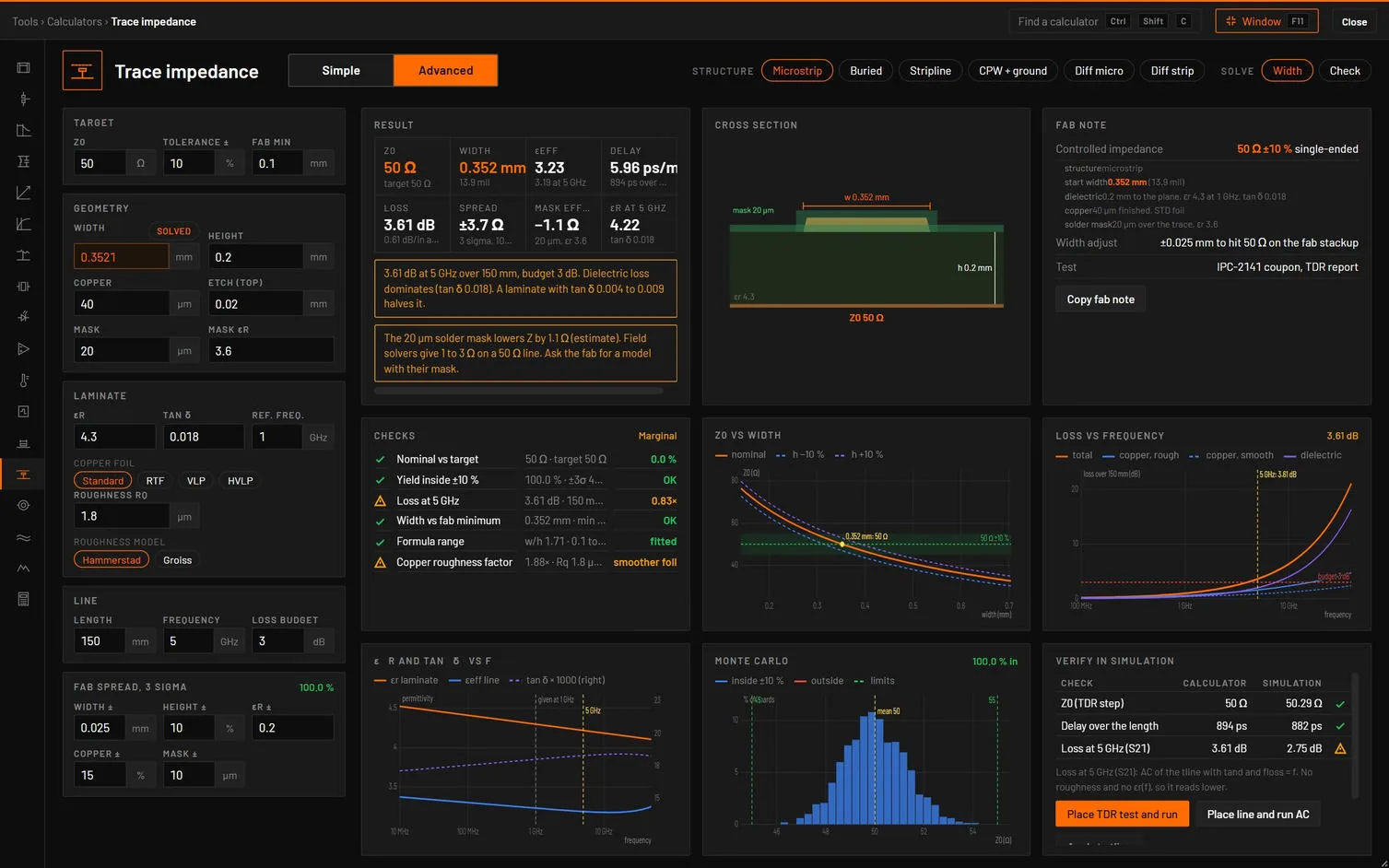
| Choice | Options | What it does |
|---|---|---|
| Structure | Microstrip, Buried, Stripline, CPW + ground, Diff micro, Diff strip | Loads typical geometry and target. |
| Solve | Width, Check |
| Tab | Its dot | Cards |
|---|---|---|
| Design | Nominal vs target, width, formula range. | Result, Cross section, Z0 vs width, Fab note, Checks. |
| Loss | Loss and roughness. | Loss vs frequency, Loss at 5 GHz. |
| Material | None. | εr and tan δ vs f, Dispersion. |
| Tolerance | Yield. | Monte Carlo, Sensitivity, Checks. |
| Verify in simulation | None. | Calculator vs simulation. |
| Field | Unit | Default | What it does |
|---|---|---|---|
| Z0 (Zdiff), Tolerance ±, Fab min | Ω, %, mm | 50, 10, 0.1 | Group Target. |
| Width, Gap, Height, Copper | mm, mm, mm, µm | SOLVED, 0.2, 0.2, 40 | Group Geometry. Gap for pairs and CPW. |
| Etch (top), Cover, Mask, Mask εr | mm, mm, µm | 0.02, 0.15, 20, 3.6 | The etch makes a trapezoid. Cover for buried. Mask on the surface types. |
| εr, tan δ, Ref. freq. | , , GHz | 4.3, 0.018, 1 | Group Laminate. |
| Copper foil, Roughness Rq, Roughness model | , µm | Standard (1.8 µm), RTF (0.8), VLP (0.5), HVLP (0.25), Hammerstad or Groiss | |
| Length, Frequency, Loss budget, Skew budget | mm, GHz, dB, ps | 150, 5, 3, 5 | Group Line. Skew for pairs. |
| Width ±, Height ±, εr ±, Copper ±, Mask ± | mm, %, , %, µm | 0.025, 10, 0.2, 15, 10 | Group Fab spread, 3 sigma, badge the yield. |
How it works it out. The engine’s own line formulas, the same code as the line parts: Hammerstad-Jensen microstrip, Wheeler stripline, a conductor-backed CPW by conformal mapping, Kirschning-Jansen and Cohn coupled lines. The calculator adds the mask or cover as a blend of the field’s air share (an estimate), the etch as the mean width, Djordjevic-Sarkar εr(f) and tan δ(f) from the pair at the reference frequency, Kirschning-Jansen dispersion of εeff, Hammerstad or Groiss roughness (saturating at 2 ×), and the loss 8.686 (αc rough + αd). The Monte Carlo draws 1500 boards with each ± entry as a 3σ limit, and the two lines of a pair etch together.
| Result | What it is |
|---|---|
| Z0 or Zdiff | Against the target, with Zodd and Zcm for a pair (orange). |
| Width | mm and mil (orange in Width mode). |
| εeff, Delay, Loss | Static and at the frequency, ps/mm and over the length, dB and dB/inch. |
| Spread | ±3σ in Ω, and the yield. |
| Mask effect or Cover effect, εr at 5 GHz | The impedance drop, and the laminate at the frequency. |
The Fab note card writes what to send the fabricator: controlled impedance with its tolerance, the structure, the start width and gap, the dielectric, copper and mask, the width adjustment allowed, and an IPC-2141 coupon with a TDR report, with Copy fab note. Sensitivity moves each spread to its 3σ limit alone.
| Check | Value and limit | Passes | Marginal | Fails |
|---|---|---|---|---|
| Nominal vs target | % | Within 2 % | Within 5 % | More |
| Yield inside ±10 % | % of boards | 99.7 % or more | 95 % or more | Less: tighten |
| Loss at 5 GHz | dB · budget | Within it | Up to 1.25 × it | More |
| Width vs fab minimum | width | At or over | Too thin | |
| Formula range | w/h (and s/h) | 0.1 to 20 (pairs 0.1 to 10) | Outside: fitted | |
| Copper roughness factor | K | 1.6 or less | More: smoother foil | |
| Coupling, Skew budget (pairs) | k and Zcm, the length mismatch allowed | (information) | ||
| Copper vs gap (CPW) | copper · 0.3 × gap | Under | Over: Z0 high |
| Message | When it shows |
|---|---|
| "No width reaches … Ω with this height and εr. Use a thinner dielectric." | No width between 2 % and 40 × the height gives the target. |
| "86.1 % of boards inside ±5 %. Largest share: width (±0.025 mm, −7.8 Ω). Tighten the width tolerance or widen the impedance tolerance." | Yield under 99.7 %. |
| "3.61 dB at 5 GHz over 150 mm, budget 3 dB. Dielectric loss dominates (tan δ 0.018). A laminate with tan δ 0.004 to 0.009 halves it." | Over the loss budget (or: Copper loss dominates. Use a wider line or a smoother foil.). |
| "The 20 µm solder mask lowers Z by 1.1 Ω (estimate). Field solvers give 1 to 3 Ω on a 50 Ω line. Ask the fab for a model with their mask." | Mask on a surface line. |
| "The … cover lowers Z0 by … Ω against the bare microstrip. Estimate from the IPC-2141 cover blend. Confirm with the fab field solver." | Buried. |
| "Pair model: Kirschning-Jansen and Cohn coupled lines, as in the engine tline_diff. Within a few % of a field solver for 0.1 ≤ w/h and s/h ≤ 10." | Pairs. |
| Check | Analysis and measurement | Limit |
|---|---|---|
| Z0 (TDR step), Zdiff for a pair | Transient: a step from 50 Ω into the line, open at the end. The input plateau reads Z/(50 + Z) | ±1.5 % of Z. The engine has no mask or etch |
| Delay over the length | The far end rises after the delay | Within 3 % |
| Loss at 5 GHz (S21) | AC of the matched line. The engine has no roughness or εr(f), so it reads lower | Between the calculator’s and the engine’s loss |
| Button | What it does |
|---|---|
| Place TDR test and run | A pulse behind 50 Ω into the line (the engine’s microstrip, stripline or CPW variant, or an ideal line for a buried line or a pair’s odd mode), open at the far end, a transient of 6 delays. Z0 plateau at the input, Far end before the delay and Far end after the delay. |
| Place line and run AC | The line matched at its own Z0 and an AC sweep. Line loss at 5 GHz. |
| Apply to tline | The structure and geometry into the selected line parts. |
| Simple | Advanced |
|---|---|
| Trace width, Dielectric height, Copper thickness, Dielectric εr, Spacing, Cover, Target impedance, Line length | Width, Height, Copper, εr, Gap, Cover, Z0, Length |
| Structure | Structure (Advanced adds CPW + ground) |
- Open Trace impedance, press Advanced: 50 Ω ±10 %, 0.2 mm, 40 µm copper with 0.02 mm etch, 20 µm mask, εr 4.3 and tan δ 0.018 at 1 GHz, standard foil, 150 mm at 5 GHz with a 3 dB budget.
- Press Place TDR test and run.
You should seeWidth 0.3521 mm for 49.998 Ω (51.08 Ω without the mask), εeff 3.233, 5.958 ps/mm. The loss is 3.61 dB against 3 dB: amber, dielectric loss dominates. Roughness 1.88 ×: amber. The Monte Carlo gives ±3σ 46.3 to 53.8 Ω, 100 % inside ±10 %. The TDR plateau reads 0.500 V for 50 Ω and the far end rises after 894 ps: both pass.
Sources. Hammerstad and Jensen (IEEE MTT-S 1980), Wadell, Transmission Line Design Handbook (1991), Cohn (1955), Wheeler (1978), Kirschning and Jansen (1982, 1984), IPC-2141, Djordjevic-Sarkar, Hammerstad and Groiss roughness. The tests check microstrip, stripline, CPW and pairs against bspice tline-calc to four digits, the roughness factor, the mask effect, the Monte Carlo, and the TDR and AC runs against bspice.