
Via current and parasitics
A plated via: its resistance, inductance and capacitance, the current it carries, its thermal resistance, and how many a current needs. The Advanced view adds through, blind and microvias with their fill, the IPC fabrication rules (land, plating, aspect ratio), a thermal-via array under a power pad, the stub resonance against a data rate with back-drilling, and inserts the via into a wire of your circuit. Group PCB. Search words include via, plated, hole, barrel, parasitic, inductance, capacitance and thermal.
The window, the Simple and Advanced views, full screen and the place buttons are in The calculator window.
62.1Simple: one via or n
| Choice | Options | What it does |
|---|---|---|
| IPC-6012 class | Class 2, Class 3 | The plating the class asks for: 20 µm or 25 µm average. |
| Field | Unit | Default | What it does |
|---|---|---|---|
| Hole diameter (finished) | mm, mil | 0.3 mm | |
| Plating thickness | µm, mil | 25 µm | |
| Via length (board thickness) | mm, mil | 1.6 mm | |
| Pad diameter, Antipad diameter | mm, mil | 0.6, 1.0 mm | |
| Board εr | 4.5 | ||
| Current | A, mA | 2 A | Reads the measured RMS current of a selected wire or part. |
| Temperature rise, Ambient | °C | 10, 25 | |
| Vias in parallel | 1 (solved) | SOLVE, solved when the calculator opens: the number the current needs. |
Barrel area A = πt(d + t), R = ρ(T) h / A, L = 5.08 h [ln(4h/d) + 1] nH and C = 1.41 εr T D1 / (D2 − D1) pF (Johnson and Graham, lengths in inches), Rθ = h / (kA) with k = 385 W/mK, and the current per via from IPC-2221 on the barrel section. n vias divide R, L and Rθ and add their C. Z = √(L/C).
| Result | What it is |
|---|---|
| Resistance | Of n in parallel (orange). |
| Inductance, Capacitance | Of n vias. |
| Current per via, Vias needed | |
| Voltage drop, Thermal resistance | |
| Via Z | √(L/C) of one via. |
| Message | When it shows |
|---|---|
| "The antipad must be larger than the pad, or the capacitance has no meaning." | Antipad at or under the pad: the capacitance then reads negative and Via Z reads –. |
| "The pad is smaller than the plated hole." | |
| "Aspect ratio over 10 to 1. Plating in a hole this deep is hard to make, so ask the fabricator or use a larger hole." | |
| "The inductance formula assumes a via longer than it is wide." | |
| "… A per via is more than one via carries for +10 °C. Use … or more." | Too few vias typed. |
| "Plating 10 µm is under the IPC-6012 class 3 average of 25 µm. Specify at least 25 µm in the hole." |
Drawings: the via from above (antipad, pad, plating, hole) and the barrel in cross section. Add the via R and L in series and run (with a straight wire of 8 grid units selected) puts R_VIA and L_VIA into it, in the live view, with no measurements.
- Open Via current and parasitics (type
via): 0.3 mm hole, 25 µm, 1.6 mm, 2 A, +10 °C.
You should seeOne via carries 1.9 A, so 2 are needed: 572 µΩ, 1.14 mV, 650 pH (1.3 nH for one), 1.2 pF, 81.4 K/W, Via Z 46.6 Ω.
62.2Advanced: through, blind and micro
| Choice | Options | What it does |
|---|---|---|
| Via | Through, Blind, Microvia | Loads typical geometry: through 0.3 mm, 25 µm, 1.6 mm, pad 0.6, antipad 1.0, drill allowance 0.1 mm. Blind 0.2 mm, 20 µm, 0.4 mm. Microvia 0.1 mm, 15 µm, 0.08 mm. |
| Fill | Open (or tented), Epoxy (plugged), Paste (conductive), Copper (filled) | Thermal k 0, 0.5, 3.5, 385 W/mK. |
| Tab | Its dot | Cards |
|---|---|---|
| Current | Current, and vias against the trace. | Result, Temperature rise vs current, Fab spec. |
| Thermal pad | Pad rise, fill, hole spacing. | Thermal pad, θ vs pitch, Checks. |
| Fabrication | Aspect ratio, plating, land, antipad. | Cross section, Fabrication checks, Land size (IPC-2221). |
| Stub | Stub resonance. | |S21| with stub, Signal. |
| Verify in simulation | None. | Calculator vs simulation. |
| Field | Unit | Default | What it does |
|---|---|---|---|
| Hole (finished), Plating, Length, Pad, Antipad, εr | mm, µm, mm, mm, mm | 0.3, 25, 1.6, 0.6, 1.0, 4.3 | Group Via. |
| Current, Rise allowed, Ambient | A, °C, °C | 4, 20, 50 | Group Current, badge the vias needed. |
| Trace width, Trace copper | mm, µm | 2.5, 47.9 | The trace the vias feed: they should carry what it carries. |
| Pad length, Pad width, Pitch, Power, Laminate k | mm, mm, mm, W, W/mK | 3, 3, 1, 1.5, 0.3 | Group Thermal pad. |
| Drill over hole, Hole tol. ±, Ring min | mm | 0.1, 0.05, 0.05 | Group Fabrication. |
| IPC-6012 class, IPC-2221 fabrication allowance | Class 2 or 3, A 0.4, B 0.25, C 0.2 mm | ||
| Data rate, Layer depth, tan δ | Gb/s, mm | 25, 0.2, 0.02 | Group Signal. |
| Back-drill, Stub left, Line Z0 | , mm, Ω | No, 0.2, 50 |
How it works it out. The current per via uses the IPC-2152 fit on the barrel unrolled as an outer trace of width π(d + t), on the safe side (vias run cooler), and the vias needed is the current over that, rounded up. The trace match is the number of vias that carry what the entered trace carries at the same rise. The barrel impedance is 60/√εr ln(antipad / (d + 2t)), a coax in the antipad. The stub is the barrel below the signal layer (or what back-drilling leaves), with its notch at c / (4 l √εr) against the Nyquist frequency, half the data rate. The thermal array fits as many vias as the pitch allows in the pad, each a barrel and its fill, in parallel with the laminate between them. The minimum land is a + 2b + c: hole and tolerance, twice the ring, and the fab allowance.
| Result | What it is |
|---|---|
| Vias needed | With the current each (orange). |
| Resistance, Drop | Of n vias at their temperature. |
| IPC-2221 current | Per via, the older chart. |
| Inductance, Pad C, Barrel Z | |
| Stub notch | Amber under 3 × the Nyquist frequency. |
| Vias in pad, Board θ, Rise | On the Thermal pad card. |
| Check | Value and limit | Passes | Marginal | Fails |
|---|---|---|---|---|
| Current, 2 vias | I · per via × n | Within it | Up to 1.11 × it | More |
| Vias vs trace | n · the trace’s match | n ≥ match | Fewer: use the match | |
| Aspect ratio (drill) | x : 1 | 8 or less (microvia 0.75) | 10 or less: advanced (microvia 1) | More: too deep |
| Plating thickness | plating · class average | At or over | 90 % or more | Thin |
| Pad (IPC-2221 land) | pad · minimum land | At or over | 95 % or more | Breakout |
| Antipad clearance | (antipad − pad)/2 · 0.15 mm | At or over | 80 % or more | Tight |
| Stub resonance | notch · Nyquist | 3 × or more | 2 × or more | Less |
| Thermal pad rise | rise · n vias, power | 20 °C or less | Up to 28.6 °C | More |
| Via fill in pad | fill | Filled or tented | Open: solder wicking | |
| Hole spacing | wall to wall · 0.2 mm | At or over | 90 % or more | Too close |
| Message | When it shows |
|---|---|
| "… needs … vias of this size for +20 °C." | Too few. |
| "The 2.5 mm trace carries 5.86 A at the same rise. Use 3 vias to match it." | Fewer than the trace match. |
| "1.4 mm stub resonates at 25.8 GHz, 2.1× the 12.5 GHz Nyquist frequency of 25 Gb/s. Back-drill to 0.2 mm (181 GHz), route on a layer near the bottom, or use a blind via." | Notch under 3 × Nyquist. |
| "Aspect ratio 8.0 : 1 exceeds 8 : 1. Plating thins in the middle of the hole. Use a hole of 0.3 mm or larger." | |
| "Pad 0.6 mm is under the IPC-2221 minimum of 0.65 mm (hole + tolerance + 2 × ring + level C allowance). Drill wander can break out. Use a 0.65 mm pad." | |
| "IPC-6012 class 2 requires 20 µm average plating in the hole." | |
| "Open vias in a thermal pad wick solder from the joint. Tent, plug, or fill and cap them (IPC-4761 type VII), or place them at the pad edge." | Fill Open. |
| Check | Analysis and measurement | Limit |
|---|---|---|
| Drop at 4 A | Operating point of R_VIA and L_VIA in the selected wire | Equal |
| Spike for 1 A/ns | L/n × 1 A/ns, a transient with a fast current step | |
| Stub notch | AC of a 50 Ω line with an open ideal line as the stub (barrel Z, delay from the stub length) | At the quarter wave |
| Thermal pad rise | Not simulated: set rth_ja on the part to the K/W for self-heating |
| Button | What it does |
|---|---|
| Insert in wire and run | R_VIA (n in parallel, at temperature) and L_VIA (L/n) in the selected wire. See below. |
| Place stub test and run AC | A 50 Ω source and load with the stub as an open ideal line, swept past the notch. Via stub loss at half the notch within ±0.1 dB, and Via stub notch under −15 dB. Greyed when there is no stub. |
| Apply θ to part | The thermal pad’s K/W as rth_ja on the selected parts. |
Insert in wire and run puts the via into your circuit: select a straight wire first (horizontal or vertical, at least 4 grid units long, 8 for the via’s two parts). The part goes in series at the middle of the wire, 4 grid units long, and the wire is split at its pins. It is a resistor R_VIA with copper’s tempco (tc1 0.00393, tnom 20 °C) at the worst-corner temperature, so it has the calculator’s hot resistance. Then the live view runs, an operating point is taken, and two measurements are added: current against the calculator (PASS up to the design current) and drop, % of the calculator’s (PASS up to 100.1 %). A wire that carries more than the design current fails both. It is one undo step, and a name in use becomes R_VIA2. The button’s tooltip asks for a wire at least 8 grid units long in all three, while the trace and wire need only 4.
| Simple | Advanced |
|---|---|
| Hole, Plating, Via length, Pad, Antipad, Board εr | Hole, Plating, Length, Pad, Antipad, εr |
| Current, Temperature rise, Ambient, IPC-6012 class | Current, Rise allowed, Ambient, IPC-6012 class |
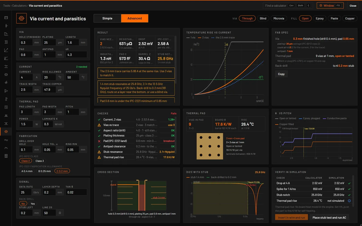
- Open Via current and parasitics, press Advanced: through, open, 4 A, +20 °C, a 3 × 3 mm pad with 1 mm pitch and 1.5 W, 25 Gb/s on a layer 0.2 mm deep.
You should see2 vias (2.53 A each): 0.631 mΩ, 2.52 mV, 1.30 nH each, 573 fF, barrel Z 30.4 Ω. Four rows are amber and one red: the 2.5 mm trace would need 3 vias, the 1.4 mm stub notches at 25.8 GHz (2.1 × the 12.5 GHz Nyquist, back-drill to 0.2 mm), the 9-via pad rises 26.4 °C, the open vias wick solder, and the 0.6 mm pad is under the 0.65 mm minimum land.
Sources. Johnson and Graham, High-Speed Digital Design (vias), IPC-2221 (current and land), IPC-2152 (the barrel as a trace), IPC-6012 (plating), IPC-4761 (via fill), IPC-2226 (microvia capture pad), the quarter-wave stub. The tests check the barrel R and θ, Johnson’s 1.18 nH for a 0.062 × 0.016 inch via, IPC-2221 and the unrolled IPC-2152 within 3 %, the land, plating, aspect ratio and pad array, the notch, and the placed R_VIA and stub test against bspice.