
dB and unit converter
Levels, ratios and prefixes. The Simple view converts between dBm, dBW, dBV, dBu, dBµV, volts and watts into an impedance, ratios and decibels both ways, and SI prefixes. The Advanced view is an RF and signal-chain toolkit: levels in twelve units with a crest factor, level sums, the noise floor and sensitivity, a gain chain with its noise figure and intercept, a free-space link budget, an ADC’s SNR, and the mismatch of a load. Group Units. Search words include db, decibel, dbm, dbv, dbu, rms, peak, watts, ratio, gain, prefix and convert.
The window, the Simple and Advanced views, full screen and the place buttons are in The calculator window.
65.1Simple: levels, ratios and prefixes
| Choice | Options | What it does |
|---|---|---|
| Convert | Levels, Ratio and dB, SI prefixes | |
| Unit | dBm, dBW, dBV, dBu, dBµV, V rms, V peak, V peak to peak, W | Levels: the unit of the value typed. |
| Ratio of | Voltage (20 log), Power (10 log) | Ratio and dB. |
| Field | Unit | Default | What it does |
|---|---|---|---|
| Value | (the unit chosen) | 0 | Levels. From a selected part it is its rms voltage: pick V rms. |
| Impedance | Ω, kΩ | 50 Ω | Levels. |
| Ratio | × | 2 | Ratio and dB. SOLVE. |
| Decibels | dB | 6.0206 (solved) | Ratio and dB. SOLVE, solved when the tab opens. |
| Value | T … f | 4700 (k) | SI prefixes, with a prefix menu. |
dBm is 10 log10 of the power over 1 mW and dBW over 1 W. dBV is 20 log10 of the voltage over 1 V rms, dBu over 0.7746 V rms (the voltage across 600 Ω at 1 mW), dBµV over 1 µV. P = V²/Z. Peak and peak-to-peak values are for a sine (√2 and 2√2 × rms).
| Result | What it is |
|---|---|
| Levels | Every unit except the one typed, with V rms in orange (or dBm when V rms is typed), and a table All levels into 50 Ω. |
| Ratio and dB | The dB (or the ratio), the same ratio taken with the other law, and the power or voltage ratio, with a table of common values from −60 to +60 dB. |
| SI prefixes | The engineering form (4.7 k) and the value in every prefix. |
| Message | When it shows |
|---|---|
| "Voltage levels do not depend on the impedance. Watts and dBm do, so check the impedance." | dBu, dBV or dBµV typed. |
| "A power of zero or less has no level in dB. Enter a power above 0 W." | W at 0 or less (volts likewise). |
| "Impedance must be above zero. Enter a value above 0 Ω." | |
| "A ratio has to be above zero." |
There are no place buttons in this view.
- Open the dB converter (type
dbm): 0 dBm into 50 Ω. - Choose V rms, type
1and Impedance600.
You should see0 dBm is 223.6 mV rms, 316.2 mV peak, 632.5 mV p-p, −13.01 dBV, −10.79 dBu, 107 dBµV, 1 mW. 1 V rms into 600 Ω is 2.218 dBm and 2.218 dBu, 0 dBV, 120 dBµV, 1.667 mW. A voltage ratio of 2 is 6.021 dB (3.01 dB as power).
65.2Advanced: noise, chains, links, ADCs and mismatch
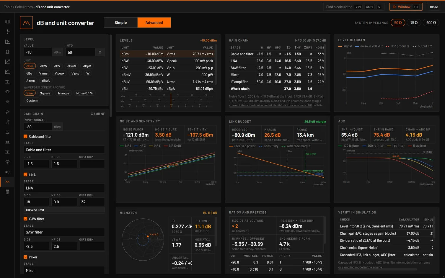
| Choice | Options | What it does |
|---|---|---|
| System impedance | 50 Ω, 75 Ω, 600 Ω | The Z0 of the chain, the mismatch and the placed circuits. It also sets the level’s Into impedance. |
| Tab | Its dot | Cards |
|---|---|---|
| Levels | None. | Levels (twelve units and the ruler). |
| Ratios and prefixes | None. | Ratios and prefixes. |
| Noise and sensitivity | Green when the SNR at the input signal reaches the SNR needed, else amber. | Noise and sensitivity. |
| Gain chain | Green when the SNR out reaches the SNR needed, else red. | Gain chain, Level diagram. |
| Link budget | Green with the fade margin and the EIRP within its limit, amber with a margin over 0, red under 0. | Link budget. |
| ADC | Green when the ADC adds 0.5 dB or less to the NF, amber up to 2 dB, else red. | ADC. |
| Mismatch | Green with a return loss of 15 dB or more, amber 10 dB or more, else red. | Mismatch. |
| Verify in simulation | None. | Calculator vs simulation. |
| Field | Unit | Default | What it does |
|---|---|---|---|
| Value, Into | (unit), Ω | −10, 50 | Group Level. |
| Unit | dBm, dBW, dBV, dBmV, dBµV, dBu, V rms, V peak, V p-p, W, A rms, dBµA | ||
| Waveform (crest factor) | Sine (1.4142), Square (1), Triangle (1.7321), Noise 0.1 % (3.29), Custom | Peak = crest factor × rms. | |
| Decibels, Ratio, Voltage or Power | dB, × | 6.0206, SOLVED | Group Ratios and prefixes. Also Level A and Level B (−10, −13 dBm) and an SI prefix value. |
| Bandwidth, SNR needed, Temperature, Resistor | kHz, dB, K, Ω | 200, 10, 290, 1000 | Group Noise and sensitivity. Noise figure from the Gain chain or Manual (NF 3 dB). |
| Input signal | dBm | −80 | Group Gain chain, badge the chain NF. |
| Stages 1 to 6 | G dB, NF dB, OIP3 dBm | Cable and filter −1.5 / 1.5, LNA 18 / 0.9 / 32, SAW filter −2.5 / 2.5, Mixer −7 / 7.5 / 15, IF amplifier 30 / 4 / 40 | Each with a tick and a name. Passive parts: NF = loss, OIP3 no limit. |
| Transmit power, EIRP limit, TX antenna, TX cable loss, RX antenna, RX cable loss | dBm, dBm, dBi, dB, dBi, dB | 14, 16.15, 2.15, 1, 2.15, 1 | Group Link budget, badge the margin. |
| Frequency, Distance, Fade margin | MHz, km, dB | 868, 2, 10 | |
| Resolution, Sample rate, Signal bandwidth, Input frequency | bits, MHz, MHz, MHz | 12, 100, 5, 30 | Group ADC. |
| Clock jitter, Datasheet SNR, Full scale, Input impedance | ps, dBFS, Vpp, Ω | 1, 66, 1, 100 | |
| Load R, Load X, Source |Γ| | Ω, Ω | 75, 25, 0.1 | Group Mismatch. |
How it works it out. The noise floor is kT + 10 log B (−173.98 dBm/Hz at 290 K) and the sensitivity adds the NF and the SNR needed. The chain’s NF is Friis (F = F1 + (F2 − 1)/G1 + …), its input IP3 from 1/IIP3 = Σ Gbefore/IIP3k (coherent, worst case), the SFDR ⅔ (IIP3 − floor). The link uses the free-space path loss 20 log(4πdf/c) and the Fresnel radius 8.66 √(dkm/fGHz) m. The ADC’s SNR combines quantisation (6.02 N + 1.76), jitter (−20 log(2π fin tj)) and the datasheet figure, adds the process gain 10 log(fs / 2 BW), and turns the floor into a noise figure in its input impedance. Mismatch: Γ = (Z − Z0)/(Z + Z0).
| Result | What it is |
|---|---|
| Levels | All twelve units, a ruler with the dBm, dBV, dBu and dBµV scales lined up, and the note In 50 Ω: dBµV = dBm + 107.0. (75 Ω: dBmV = dBm + 48.75). |
| Ratios | The dB as power and voltage, the power sum of two levels, their coherent sum and difference, and the engineering form. |
| Noise | Noise floor, Noise figure, Sensitivity, Noise temperature, Resistor noise (√4kTR) and Noise in B, with a plot of sensitivity against bandwidth for NF 1, 3, 6 and 10 dB. |
| Gain chain | A table per stage: G, NF, IIP3, the running gain, NF and IIP3, and each stage’s share of the noise and of the IM3, with the whole chain. The level diagram draws the signal, the noise, the IM3 products and the output IP3 along the chain. |
| Link | Received, Margin, Range (with the fade margin kept), EIRP, Fresnel zone and the path loss slope, with received power against distance. |
| ADC | SNR at Nyquist, ENOB, SNR in band, noise density, the ADC’s noise figure and the chain + ADC NF, with SNR against input frequency for jitter of 0.1 to 5 ps. |
| Mismatch | A Smith chart, |Γ|, Return loss, VSWR, Mismatch loss and the uncertainty with the source’s |Γ|, and a VSWR table. |
| Message | When it shows |
|---|---|
| "Link … dB short at …. Range with fade margin: …. Use higher-gain antennas, a lower NF or less bandwidth." | A negative margin. |
| "EIRP 21.1 dBm is above the 16.1 dBm limit." | Over the EIRP limit. |
| "ADC adds 0.6 dB to the NF. Chain noise at the ADC is 8 dB above its floor (−141.4 dBm/Hz). Add 2 dB of gain before the ADC for a 10 dB gap, or use an ADC with a lower floor." | The ADC adds over 0.5 dB. |
| "6.0 dB loss before the LNA adds 6.0 dB to the NF. Move the LNA closer to the antenna where the filtering allows." | Loss before the first active stage. |
| "Level referenced to 75 Ω. System impedance is 50 Ω." | The level’s impedance differs from the system’s. |
| "Generator levels assume a 50 Ω load. A 1 MΩ scope input reads twice the voltage (+6.02 dB)." | A level into 75 Ω or less. |
| Check | Analysis and measurement | Limit |
|---|---|---|
| Level into 50 Ω (sine, transient rms) | A generator behind Z into Z: rms and peak of V(LOAD) | ±1 %. Sine only: the crest factor of other waves is not placed. |
| Chain gain (AC, stages as gain blocks) | AC at 1 MHz: one Z0 gain block per stage | ±0.02 dB |
| Divider ratio of ZL (AC at the port) | AC at 100 MHz of the load against the source | ±0.02 dB |
| Chain noise figure (Noise) | Noise analysis: a matched pad of loss F before a noiseless block per stage | Read in the Noise view |
| Cascaded IIP3, link budget, ADC jitter | Not simulated: the engine has no intermodulation, antenna or sampling model |
| Button | What it does |
|---|---|
| Place chain, run Noise | Per stage a matched T-pad of loss F (a pad alone has NF = F) and a noiseless gain block, and a noise analysis at OUT from 100 kHz to 10 MHz. The chain NF comes out of the noise contributions in the Noise view. |
| Place chain, run AC | V1, RS = Z0, per stage RIN, a controlled source of twice the voltage gain and ROUT, then RL, and an AC sweep. Chain gain, V(OUT) against half the source = chain gain − 6.02 dB, ±0.02 dB. |
| Place source and load | A 1 kHz generator behind Z into Z, a transient of 10 periods. Load level, rms and Load level, peak, ±1 %. |
| Place mismatch, run AC | V1 at 100 MHz, RS = Z0, the load R with a series L or C for X. Divider ratio of the load = 20 log(|1 + Γ|/2), ±0.02 dB. |
The simulator runs at 27 °C, 0.15 dB above the 290 K of the NF definition in absolute floor, which cancels in the ratio.
| Simple | Advanced |
|---|---|
| Value, Impedance, Unit | Value, Into, Unit |
| Ratio, Decibels, Ratio of | Ratio, Decibels, Voltage or Power |
- Open the dB converter and press Advanced: the five default stages, −80 dBm in, 200 kHz, the 868 MHz link over 2 km, a 12-bit 100 MS/s ADC.
- Read the Gain chain, Link budget and ADC tabs.
You should seeThe chain has 37.0 dB gain, NF 3.50 dB (1.50, 2.40, 2.44, 2.88, 3.50 along it) and IIP3 1.6 dBm: SFDR 79.4 dB, SNR out 37.5 dB. The link receives −80.9 dBm after 97.2 dB path loss: 26.5 dB margin, 13.4 km range, Fresnel radius 13.1 m. The ADC gives 65.4 dB at Nyquist (10.6 bits ENOB) and 75.4 dB in band, but adds 0.64 dB to the NF: amber, with the advice to add 2 dB of gain before it. The 75 + j25 Ω load has |Γ| 0.277, return loss 11.1 dB (amber), VSWR 1.77. Place chain, run AC passes at 30.98 dB.
Sources. The standard definitions of the units, Friis for the noise figure and the path loss, the cascade formula for the intercept, 6.02 N + 1.76 and the aperture-jitter limit for ADCs. The tests check levels into 50 Ω (0 dBm is 223.6 mV, dBµV = dBm + 107), a two-stage NF of 3.953 dB, pad NF = loss, the SFDR, the path loss 32.44 + 20 log dkm + 20 log fMHz, the 75 + j25 mismatch, and the placed chain’s noise figure in bspice within 0.01 dB.